CPU Architecture & the Fetch-Decode-Execute Cycle (OCR A-Level CS 1.1.1)
OCR A-Level CS 1.1.1 explained: the CPU's ALU, control unit, registers and buses, the fetch-decode-execute cycle, and Von Neumann vs Harvard. With exam tips.

Free CPU Architecture FDE revision resources (OCR A-Level Computer Science, 1.1.1)
We’ve made exam-style practice for this exact topic, free to download: CPU Architecture FDE question sheet, mark scheme and cheat sheet. Grab them, have a go, then read the full guide below.
I'll be honest with you: 1.1.1 looks like the driest topic in the whole specification. A list of registers, three buses, a cycle that repeats a billion times a second. It reads like something to memorise and forget. But here is the thing. This is where almost every mark on Paper 1 quietly begins. Every line of code you have ever written, from a one-line Python script to a whole game engine, ends up as a stream of tiny machine-code instructions that the processor has to fetch, decode and carry out. The students who genuinely understand that process, rather than just reciting it, pick up easy marks on the same LMC question year after year, while everyone else fumbles it. So give me the next few minutes. Get this solid now and assembly language, performance and architecture all become far easier later.
This guide covers the three parts of spec point 1.1.1 you need: the components of the CPU, the fetch-decode-execute cycle, and the difference between Von Neumann, Harvard and contemporary architectures.

What are the main components of the CPU?
The central processing unit (CPU) has two working parts plus a set of registers, all wired to main memory by three buses.
The Arithmetic Logic Unit (ALU) is the calculator. It performs arithmetic such as add, subtract, multiply and divide, logical comparisons using AND, OR, NOT and XOR, and bit shifts to the left or right.
The Control Unit (CU) is the conductor. It fetches each instruction in turn, decodes the opcode to work out what it means, and sends out control signals over the control bus so that every other part acts at the right moment.
Registers are tiny, extremely fast storage cells inside the CPU itself. OCR expects you to know five by name and job:
Program Counter (PC) holds the address of the next instruction to be fetched.
Current Instruction Register (CIR) holds the instruction currently being decoded and executed, split into opcode and operand.
Memory Address Register (MAR) holds the address of the memory location about to be read from or written to.
Memory Data Register (MDR) temporarily holds the data or instruction travelling to or from memory (also called the memory buffer register, MBR).
Accumulator (ACC) holds the working value and the results coming out of the ALU.
The CPU talks to main memory over three buses. The address bus carries a memory address outward from the CPU (it is one-directional). The data bus carries data and instructions in both directions. The control bus carries timing and control signals, such as a read or write signal, from the control unit. A handy exam fact: the width of the address bus sets the maximum amount of memory the system can address (an n-line address bus can reach 2ⁿ locations).
How does the fetch-decode-execute cycle work?
You might be thinking that is a lot of parts to keep straight. Here is the reassuring bit: they only ever do one job, in one fixed order, and that order is the fetch-decode-execute (FDE) cycle, the loop the CPU repeats billions of times a second, processing one instruction per pass. Think of a chef working through a recipe: read the next step off the card (fetch), work out what it is actually asking for (decode), then do it (execute), and move on to the next line.
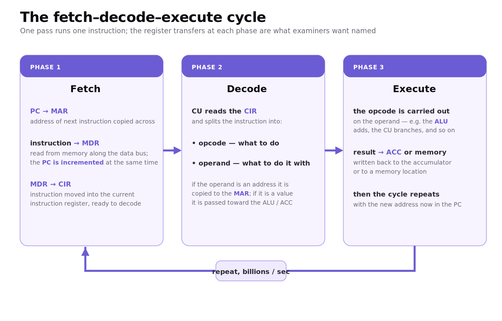
Fetch. 1. The address in the PC is copied to the MAR. 2. The instruction at that address is sent along the data bus into the MDR. At the same time, the PC is incremented so it points at the next instruction. 3. The contents of the MDR are copied into the CIR.
Decode. 4. The control unit decodes the instruction in the CIR, splitting it into the opcode (what to do) and the operand (what to do it with). If the operand is an address, it is copied to the MAR ready for the next read; if it is a value, it is passed towards the ALU or accumulator.
Execute. 5. The opcode is carried out on the operand. The result is written back, usually to the accumulator or to a memory location, and the cycle starts again with the new value in the PC.
Worked example: tracing one instruction
Suppose the PC holds 08, and memory location 08 contains the instruction ADD 20 (add the contents of address 20 to the accumulator).
Fetch: PC (08) → MAR. Memory[08] = "ADD 20" → MDR, and PC becomes 09. MDR → CIR.
Decode: CIR splits into opcode ADD and operand 20. Because 20 is an address, it is copied to the MAR.
Execute: Memory[20] is read into the MDR, the ALU adds it to the value already in the accumulator, and the answer is stored back in the accumulator.
This is the most important part, so do not skim it: the PC moved to 09 during the fetch, not at the end. That one detail is worth easy marks every single year, and it is the thing students get wrong time and time again. Learn it once, properly, and it is yours.
What is the difference between Von Neumann, Harvard and contemporary architecture?
These three terms (spec point 1.1.1e) all answer one question: how does the CPU connect to its memory? Hold on to that framing and the rest falls into place.
Von Neumann architecture uses a single shared memory and a single bus system for both instructions and data: the "stored program" concept, where a program must be loaded into main memory and its instructions are fetched and executed one at a time. Almost every general-purpose PC works this way. Its weakness is the Von Neumann bottleneck: data and instructions compete for the same bus, so only one can move at a time.
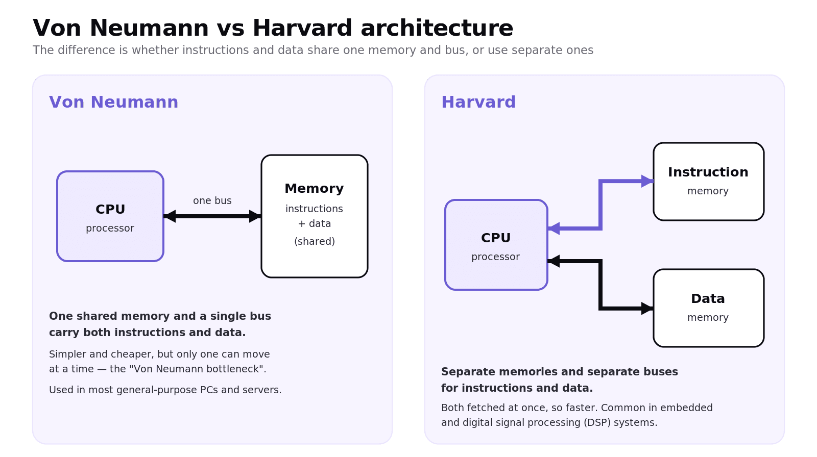
Harvard architecture uses physically separate memories and buses for instructions and data, so both can be fetched at the same time. This makes it faster but more complex, which is why it is common in embedded and digital signal processing systems (for example, instructions in ROM and data in RAM).
Contemporary architecture is a hybrid. A modern CPU has one main memory (Von Neumann style) but splits its on-chip cache into separate instruction and data caches (Harvard style) so the processor gets the parallel access benefit close to the core. That is the "feature not part of standard Von Neumann" examiners often ask you to describe.
Common exam mistakes
These are the slips I see again and again. Read them now. Catching your own mistake before the exam is far cheaper than catching it after.
Mixing up the MAR and MDR. The MAR only ever holds an address; the MDR holds the data or instruction in transit. Swapping them loses marks instantly.
Saying the PC increments at the end of the cycle. It is incremented during the fetch phase, right after the address is copied to the MAR.
Confusing the CIR with the PC. The CIR holds the current instruction; the PC holds the address of the next one.
Vague Von Neumann definitions. "It stores programs" is not enough. Say shared memory and a single bus for both data and instructions.
Forgetting bus direction. When asked, state that the address bus is one-directional (out of the CPU) while the data bus is bidirectional.
Not linking registers to the instruction. In "explain which registers are used when X executes" questions, name each register and the value it holds at that step.
Quick recap
The CPU = ALU (calculations) + Control Unit (decoding and control signals) + registers (PC, CIR, MAR, MDR, ACC).
Three buses connect CPU and memory: address (one-way), data (two-way) and control; address-bus width sets maximum addressable memory.
Fetch: PC→MAR, instruction→MDR (PC incremented), MDR→CIR. Decode: split into opcode + operand. Execute: opcode acts on operand, result to accumulator.
Von Neumann = one shared memory and bus; Harvard = separate instruction and data memories; contemporary = Von Neumann main memory with split Harvard-style cache.
Most marks are lost on MAR/MDR confusion and on when the PC increments.
And look, I know this topic can feel like rote learning, but it really is not. Trace one instruction by hand, out loud, register by register, and the whole cycle stops being a list and starts being a story you can tell. Do that two or three times and you will own these marks. Work hard now, enjoy later. I believe in you.
Frequently asked questions
What is the difference between the MAR and the MDR? The Memory Address Register holds the address of the location the CPU wants to access; the Memory Data Register holds the actual data or instruction being moved to or from that location. One carries "where", the other carries "what".
Does the program counter increment during fetch or execute? During fetch. As soon as the instruction's address has been copied to the MAR and the instruction is being read into the MDR, the PC is incremented so it already points at the next instruction.
What is the difference between the CIR and the accumulator? The CIR holds the current instruction (opcode plus operand) while it is decoded and executed. The accumulator holds data: the working value and the result produced by the ALU.
Is the fetch-decode-execute cycle the same as Von Neumann architecture? They are linked but not the same. The FDE cycle is the process of running one instruction; Von Neumann architecture is the design (shared memory and bus) that makes the stored-program FDE cycle possible.
How is 1.1.1 examined on OCR Paper 1? Very often, and usually applied. Expect short "state the register" questions, 2-4 mark "describe how the accumulator/PC is used" questions, and 4-6 mark questions asking which registers and buses are used as a given LMC instruction executes.
Why is Harvard architecture faster than Von Neumann? Because instructions and data live in separate memories on separate buses, the CPU can fetch an instruction and read or write data at the same time, avoiding the Von Neumann bottleneck where both share one bus.


